
ORT82G5-G2-PAC-EV
Сравнение
ORT82G5-G2-PAC-EV
BOARD BRIEFCASE ORT82G5 SERDES


Сравнение
Цена договорная
Обновление цены:несколько месяцев назад
В наличии:
4439


45
Обслуживание клиентов в 45 странах
1000+
Мировые производители
$140M
За пять лет рост составил 140 млн. долл. США
50.0M+
Доставка 50 миллионов за 5 лет.

Lattice Semiconductor Corporation
Компания Lattice Semiconductor является лидером в области программирования с низким энергопотреблением, решая сложные задачи в сетях, от граничных до облачных. Занимая прочные позиции в сфере коммуникаций, вычислительной техники, промышленности, автотранспорта и потребительских товаров, компания поддерживает долгосрочные отношения, предлагая поддержку мирового класса для беспрепятственного внедрения инноваций, создавая безопасный, подключенный мир.
Посмотреть все товары Lattice Semiconductor Corporation


The ORT42G5 and ORT82G5-G2-PAC-EV provide a clockless high-speed interface for interdevice communication on a board or across a backplane. The built-in clock recovery of the ORT42G5 and ORT82G5-G2-PAC-EV allows for higher system performance, easier-to-design clock domains in a multiboard system, and fewer signals on the backplane. Network designers will benefifit from the backplane transceiver as a network termination device. The device supports embedded 8b/10b encoding/decoding and link state machines for 10 G Ethernet, and Fibre Channel.
The ORT82G5-G2-PAC-EV is pinout compatible with a sister device, the ORSO82G5, which implements eight channels of SERDES with SONET scrambling and cell processing. The ORT42G5 is pin compatible with the ORSO42G5,which implements four channels of SERDES with SONET scrambling and cell processing.
Feature
• High-performance programmable logic:
– 0.16 µm 7-level metal technology.
– Internal performance of >250 MHz.
– Over 400K usable system gates.
– Meets multiple I/O interface standards.
– 1.5V operation (30% less power than 1.8V operation) translates to greater performance.
• Traditional I/O selections:
– LVTTL (3.3V) and LVCMOS (2.5V and 1.8V) I/Os.
– Per pin-selectable I/O clamping diodes provide 3.3V PCI compliance.
– Individually programmable drive capability: 24 mA sink/12 mA source, 12 mA sink/6 mA source, or 6 mA
sink/3 mA source.
– Two slew rates supported (fast and slew-limited).
– Fast-capture input latch and input Flip-Flop (FF)/latch for reduced input setup time and zero hold time.
– Fast open-drain drive capability.
– Capability to register 3-state enable signal.
– Off-chip clock drive capability.
– Two-input function generator in output path
• New programmable high-speed I/O:
– Single-ended: GTL, GTL+, PECL, SSTL3/2 (class I and II), HSTL (Class I, III, IV), ZBT, and DDR.
– Double-ended: LVDS, bused-LVDS, and LVPECL. Programmable (on/off) internal parallel termination (100
Ω) is also supported for these I/Os.
• New capability to (de)multiplex I/O signals:
– New DDR on both input and output at rates up to 350 MHz (700 MHz effective rate).
– New 2x and 4x downlink and uplink capability per I/O (i.e., 50 MHz internal to 200 MHz I/O).
• Enhanced twin-block Programmable Function Unit (PFU):
– Eight 16-bit Look-Up Tables (LUTs) per PFU.
– Nine user registers per PFU, one following each LUT, and organized to allow two nibbles to act independently, plus one extra for arithmetic operations.
– New register control in each PFU has two independent programmable clocks, clock enables, local SET/RESET, and data selects.
– New LUT structure allows flflexible combinations of LUT4, LUT5, new LUT6, 4 → 1 MUX, new 8 → 1 MUX, and ripple mode arithmetic functions in the same PFU.
– 32 x 4 RAM per PFU, confifigurable as single- or dual-port. Create large, fast RAM/ROM blocks (128 x 8 in only eight PFUs) using the Supplemental Logic and Interconnect Cell (SLIC) decoders as bank drivers.
– Soft-Wired LUTs (SWL) allow fast cascading of up to three levels of LUT logic in a single PFU through fast internal routing which reduces routing congestion and improves speed.
– Flexible fast access to PFU inputs from routing.
– Fast-carry logic and routing to all four adjacent PFUs for nibble-wide, byte-wide, or longer arithmetic functions, with the option to register the PFU carry-out.


Атрибуты продукта
| ТИП | ОПИСАНИЕ | Полная выборка |
|---|---|---|
| Серия | Серия 4 ORCA® | |
| Пакет | Насыпной | |
| Состояние продукта | Устаревший | |
| Тип | ПЛИС | |
| Для использования с/сопутствующими продуктами | ORT82G5 | |
| Содержание | Плата(ы), кабель(ы), блок питания |
Блог

 Микроконтроллеры против микропроцессоров: Раскрытие основных различий для инженерии встроенных системПрофессионалы в области разработки встроенных систем и продуктов в электронике часто сталкиваются с проблемой различения микроконтроллеров и микропроцессоров. Несмотря на их основополагающую роль в проектировании и изготовлении множества электронных устройств, понимание их уникальных функций на основе только определений может быть затруднительным:
 Глубокое погружение в мировой рынок керамических конденсаторовПрисоединяйтесь к нам в изучении развивающегося направления экологического сознания на мировом рынке керамических конденсаторов.
 Освоение измерения тока с помощью микроконтроллеровЭто исследование текущих нюансов измерения позволит раскрыть источники этих ошибок и представить супергеройское решение: встроенные аналоговые периферийные устройства, независимые от ядра (CIP).
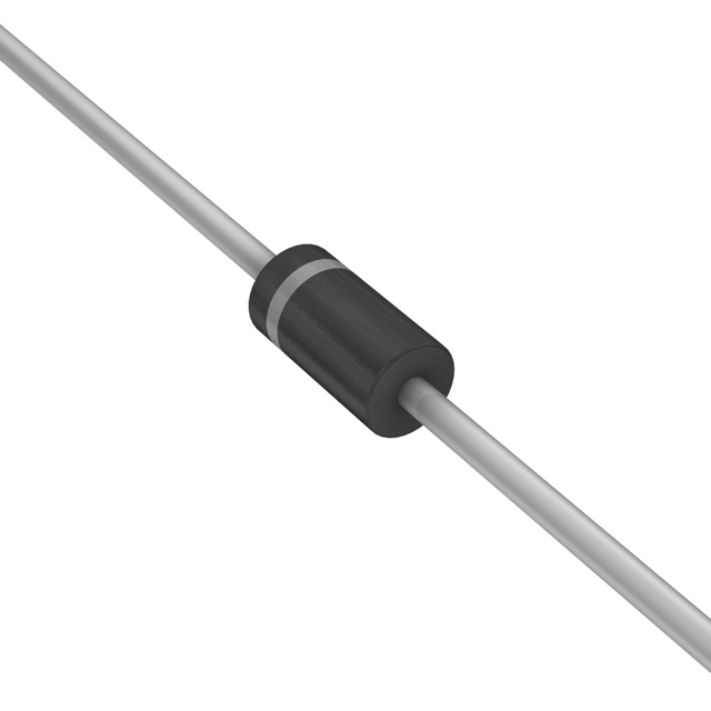 Что такое выпрямительный диод: руководство для начинающихВ этом увлекательном путешествии мы разгадаем тайны этих диодов, узнаем, что они из себя представляют, как они творят чудеса, их применение и некоторых основных участников оркестра выпрямительных диодов.
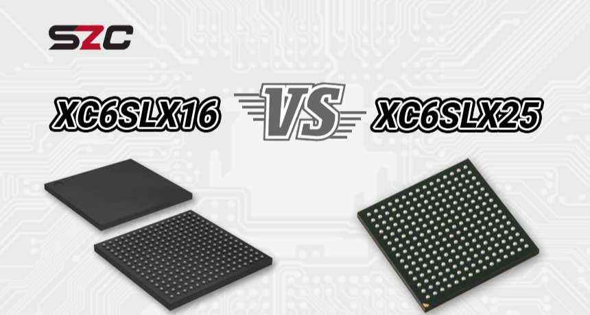 Противостояние FPGA: XC6SLX16 против XC6SLX25Откройте тайны FPGAs с помощью нашего быстрого гида! XC6SLX16 или xc6slx25 - у кого из них ключ к вашему следующему технологическому приключению? Нажмите сейчас, чтобы открыть мир программируемых возможностей!


Цена договорная
Обновление цены:несколько месяцев назад
В наличии:
4439
Lattice Semiconductor Corporation
Компания Lattice Semiconductor является лидером в области программирования с низким энергопотреблением, решая сложные задачи в сетях, от граничных до облачных. Занимая прочные позиции в сфере коммуникаций, вычислительной техники, промышленности, автотранспорта и потребительских товаров, компания поддерживает долгосрочные отношения, предлагая поддержку мирового класса для беспрепятственного внедрения инноваций, создавая безопасный, подключенный мир.
Посмотреть все товары Lattice Semiconductor CorporationБлог
- Микроконтроллеры против микропроцессоров: Раскрытие основных различий для инженерии встроенных системПрофессионалы в области разработки встроенных систем и продуктов в электронике часто сталкиваются с проблемой различения микроконтроллеров и микропроцессоров. Несмотря на их основополагающую роль в проектировании и изготовлении множества электронных устройств, понимание их уникальных функций на основе только определений может быть затруднительным:
- Глубокое погружение в мировой рынок керамических конденсаторовПрисоединяйтесь к нам в изучении развивающегося направления экологического сознания на мировом рынке керамических конденсаторов.
- Освоение измерения тока с помощью микроконтроллеровЭто исследование текущих нюансов измерения позволит раскрыть источники этих ошибок и представить супергеройское решение: встроенные аналоговые периферийные устройства, независимые от ядра (CIP).
- Что такое выпрямительный диод: руководство для начинающихВ этом увлекательном путешествии мы разгадаем тайны этих диодов, узнаем, что они из себя представляют, как они творят чудеса, их применение и некоторых основных участников оркестра выпрямительных диодов.
- Противостояние FPGA: XC6SLX16 против XC6SLX25Откройте тайны FPGAs с помощью нашего быстрого гида! XC6SLX16 или xc6slx25 - у кого из них ключ к вашему следующему технологическому приключению? Нажмите сейчас, чтобы открыть мир программируемых возможностей!
Популярные производители
View all manufactures Больше


Горячие продукты
Дополнительные электронные компоненты Больше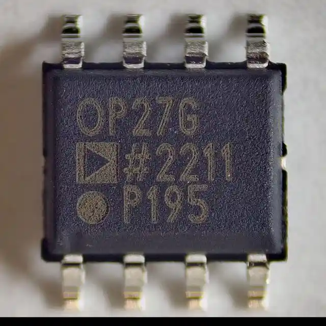
OP27GSZ-REEL
IC OPAMP GP 1 CIRCUIT 8SOIC
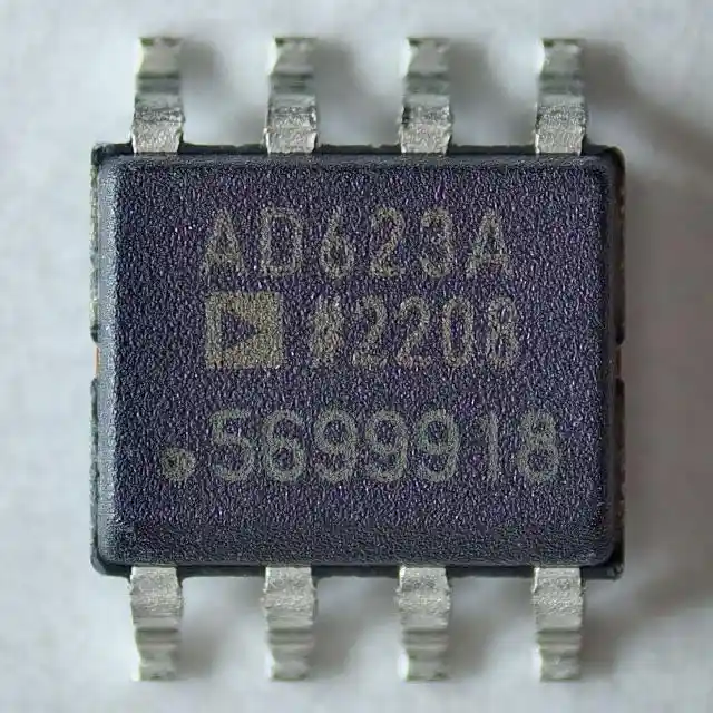
AD623ARZ-R7
IC INST AMP 1 CIRCUIT 8SOIC
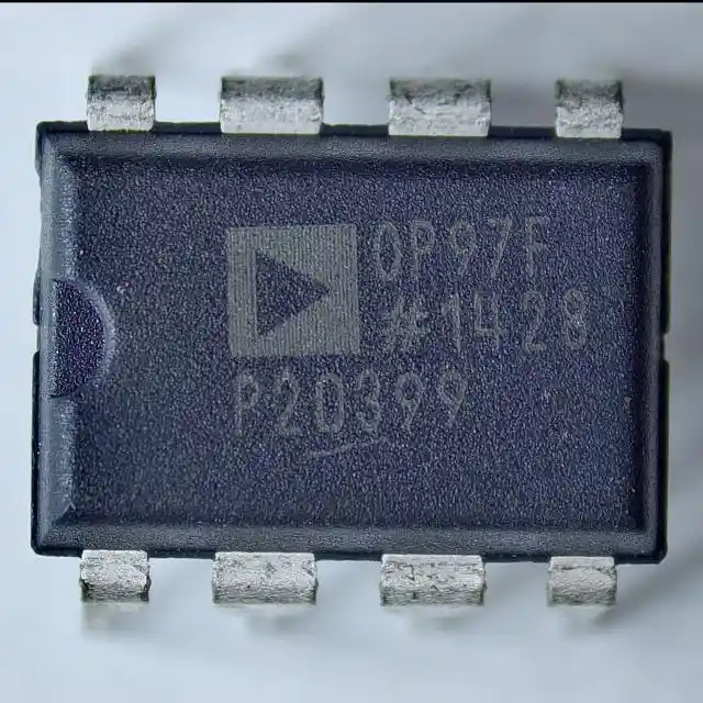
OP97FPZ
IC OPAMP GP 1 CIRCUIT 8DIP
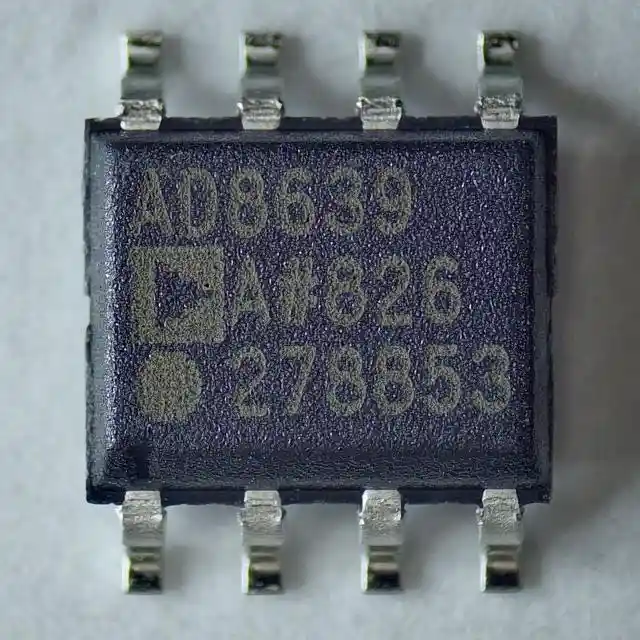
AD8639WARZ
IC OPAMP ZERO-DRIFT 2 CIRC 8SOIC
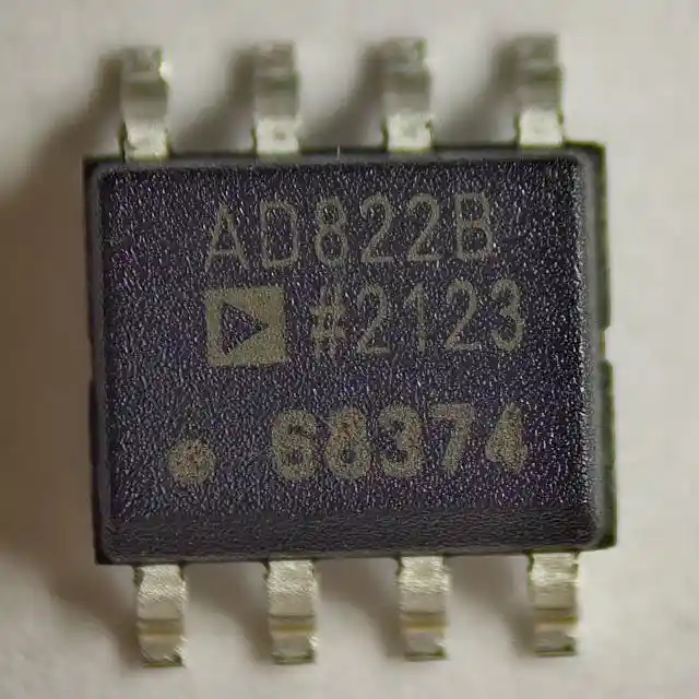
AD822BRZ-REEL7
IC OPAMP GP 2 CIRCUIT 8SOIC
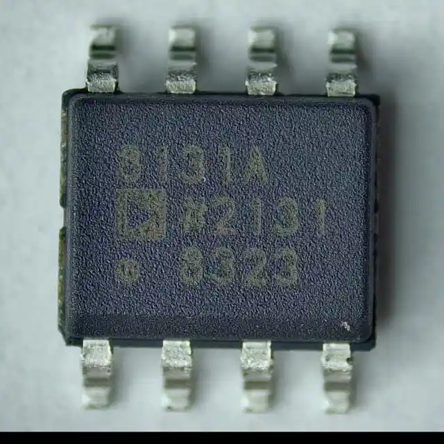
AD8131ARZ-REEL7
IC OPAMP DIFF 1 CIRCUIT 8SOIC
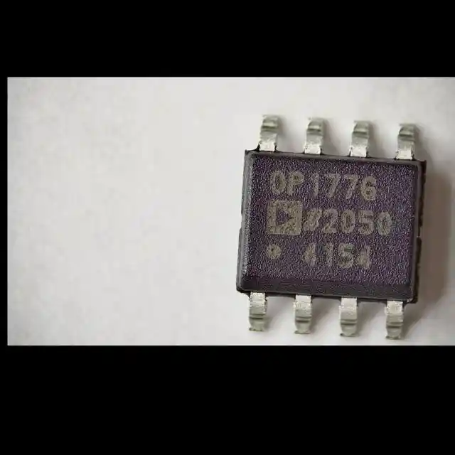
OP177GSZ-REEL
IC OPAMP GP 1 CIRCUIT 8SOIC
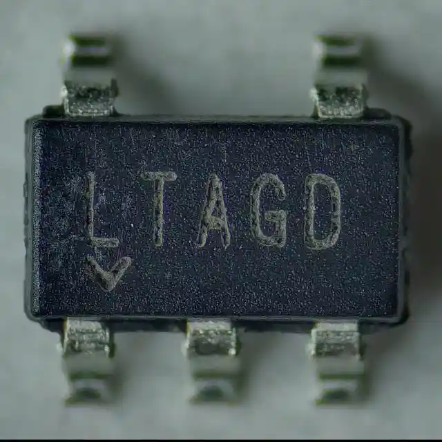
LTC2054HVIS5#TRMPBF
IC OPAMP ZER-DRIFT 1CIR TSOT23-5
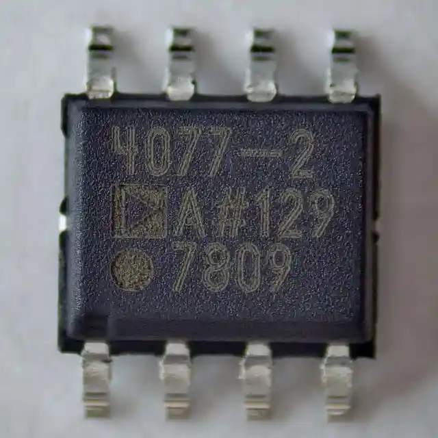
ADA4077-2ARZ-R7
IC OPAMP GP 2 CIRCUIT 8SOIC
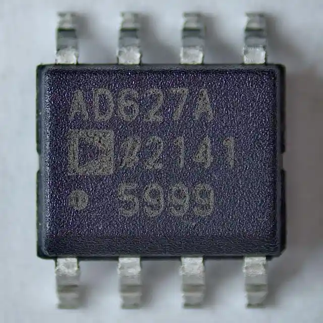
AD627ARZ-R7
IC INST AMP 1 CIRCUIT 8SOIC